
First Page |
Second Page | Third Page |
Some projects are just not feasible without a specially designed Printed Circuit Board (PCB). Simple circuits can be built using point-to-point wiring, stripboard, veroboard or other prototyping methods. However, if space is at a premium or there are many connections per net then it is desirable to assemble the circuit on its own PCB. This also improves performance and reliability, and makes the circuit easier to assemble. For more information on PCB's follow this link rather than have me bore you with all the details. It should be noted that I wrote this web page as part of a TAFE project. For this reason I have included the string A3ARMIT2009.
There are many ways to generate the PCB artwork. I won't go into too much detail about these suffice to say that while commercial layout programs are often better integrated for schematic capture and simulation, and offer more output options, there are plenty of free programs that are still very powerful in their own right. Either way, most programs I have used have component libraries that are unsuitable for single-sided non plated through hole boards, the only kind of PCB that can easily be made at home (I have not tried to make a double-sided board, nor have I needed to, since I have started to get the hang of designing single-sided PCB artwork). Generally pads must be modified to use the PCB drills you have available and the copper area must be widened to prevent the pads lifting off the board during soldering.
This page specifically talks about making printed circuit boards photographically using UV sensitive photoresist, but some mention will be made of the Dalo pen and toner transfer methods also. Both techniques basically involve having some kind etch resist in areas where we want copper artwork. Areas that we want to be free of copper are left unprotected. We then etch the board in a solution which will remove the copper from the unprotected area, whereas the protected copper will be left behind to form the PCB wiring.
In this method the copper tracks are drawn freehand on blank copper clad board, traditionally using something called a Dalo® pen. The ink of the pen resists etching, so the areas where tracks have been drawn using this pen will be unetched. Actually, most everyday marker pens will be etch resistant, such as permanent marker, CD pens and Sharpies®. Many will allow finer artwork and are easier to see than the blue ink of Dalo® pens. In fact Dalo® pens are generally more expensive and the ink often runs where you don't want it to. The only advantage as far as I can see is that it is easier to remove with solvent than the other markers.
Although this method allows a quick board without designing a layout on computer this method is prone to error. More often the artwork is copied from a magazine photocopy or computer printout. You can even design the artwork in PCB layout software, print the artwork and copy it by hand. Generally you will need to do this as even if you draw the tracks by hand as you will need the printout/photocopy as a drilling template as there is no way you will be able to make the board accurately enough by hand to hold anything but the simplest discrete devices, and IC's will be out of the question. Using the printed artwork taped directly over the board, either mark the drill holes with a centre punch and drill in a later step, or drill now using the artwork as a template. The artwork is then copied by hand using the drill holes as reference points.
If you are very careful this technique can work well for even medium complexity boards provided the component density is not too high. It is particularly good for discrete power circuits such as power supplies and amplifiers. This technique has the lowest startup cost (the cost of a marker pen and some solvent to remove it) and the lowest consumables cost (only need blank copper clad board and etchant). This is probably the quickest method for very simple circuits, although when one is practiced at the others there isn't much difference. The disadvantes are that it is easy to make a mistake, the results are inconsistent, and it is a one off only. Also it is impossible to draw the actual component pads so you can't use the artwork itself as a drilling guide. Also the resulting board is not aesthetically pleasing. Nonetheless, this is probably the best technique for beginners who want to make a board on a budget.Follow this link To see a fellow students website with good pictures and description of making and etching a simple board using this technique. More content may be added in the future.
| This is a very simple board, the artwork having been drawn by hand with a permanent marker. It has already been populated with components and soldered. Even though the layout was designed on computer the end result looks like it was designed on the back of a napkin. It is not generally possible to have tracks run close together or between the legs of components. Compare this board to the one at the top of the page, which is a similair circuit. The blotches are remnants of the permanent marker used to draw the tracks. | |
I won't go into much detail about this technique as there is a wealth of information and demonstrations on the internet, even on Youtube. Basically you laser print you artwork onto special paper, then you heat the print (which is called toner), fusing it onto the copper board, typically using a household iron. This toner forms the etch resist which makes the tracks and pads, so when you print your artwork from a computer this is what ends up on the board. The special paper can be a purpose bought product made for making PCB's, but there are many other papers that will do the job. I got best results from using magazine paper culled from junk mail in my letterbox, the only disadvantage being that some of the pictures from the flier transferred also. This had to be gently scrubbed off prior to etching.
To be perfectly honest I am not a very big fan of this technique as I could never get it to work very well for small PCB's, so I may be slightly biased. It is impossible to know if all the tracks have transferred properly until the very end and by then the only option is to scrub the board clean and start over. Also, the board has to be inspected very carefully for any breaks in the tracks and these have to be touched up by hand with an etch resist pen, which can then lead to other slips. This makes it difficult to use very narrow tracks. Also, a lot of pressure and force must be used when ironing on the toner. Inevitable the paper moves slightly in the process, leading some tracks to end up closer to some and further from others, limiting the clearances possible. I personally found the whole process frustrating, but many people swear by it, and it seems the most popular technique on the internet. Nonetheless the method can do reasonably complex circuits provided tracks and clearances aren't miniscule and will do designs that are impossible to draw freehand. The technique is still very low in cost provided you already have a laser printer, as you otherwise need the same materials as you would using the pen method. However laser printers are more expensive than inkjet printers, and inkjet printers won't work as they use ink, not toner. Also some newer budget lasers won't work either, but most older ones do apparently. If we didn't have the photographic technique this would probably be the only serious way to make boards at home.
The board below was made with the toner transfer method. Although the results are acceptable the board has been touched up in several places with a permanent marker. Also some tracks moved slightly and ended up too close together. Had the tracks and pads in the design been larger such as in a power amplifier design the artwork might not need touching and then the results would have a professional look. This board is unetched.
|
|
Why not? This was the last technique I tried as I was unsatisfied with the results I was getting with the previous methods. The reason I had not attempted this method first was because:
It is true that you have to make or buy a good UV source to do a good exposure. I made mine at very low cost as I obtained a large quantity of UV LED's for free, but there was still some time involved. Making a photo-mask with a laser printer and tracing paper is no harder than printing the artwork any other way and as we have seen is a necessary step in the previous methods anyway. Once we have a good photo-mask we can make as many boards from it as we like and only need to make a new one if we decide to change the artwork. This actually saves time because if we mess things up in either the exposure or etching stages we don't have to waste time printing the artwork again. If we are using the toner transfer message we must start all over again and reprint the artwork. The cost is slightly higher for the photographic method as we need pre-sensitised boards (or a spray on photoresist) and possibly a proprietry developer (but I used caustic soda).
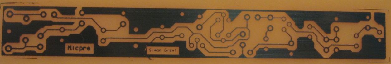
The method does require some experimentation but in reality you also need to practice the other methods quite a few times also to get usable results. If you are methodical and note down the results of your experiments, you will quickly perfect your technique. Once you have done this you will be able to reliably produce boards of less than 10/10 mil (trace width/clearance) requiring no touching up. I am still a novice at this technique and I can reliably produce images like the one at the top of the page. It is hard to get an idea of scale as the photo is hi-res but the artwork is only 12mm high and the tracks are 10 mil (1 mil = 1 thousandth of an inch). It is very hard for me to read my name on the actual board and I think I have pretty good eyesight. Below is an image of me holding the unetched board:
 |